The U.S. Department of Commerce’s (DOC) National Institute of Standards and Technology (NIST) is announcing a funding opportunity of up to $1.6 billion to support advanced semiconductor packaging research and development (R&D).
“This ambitious funding opportunity is designed to fill key technology gaps in advanced packaging to ensure U.S. leadership in the global semiconductor ecosystem,” says NIST Director Laurie E. Locascio. “CHIPS for America is delivering on its mission to create a domestic packaging industry where advanced node chips manufactured in the U.S. and abroad can be packaged within the United States.”
Supporting the DOC’s CHIPS for America initiative, this notice of funding opportunity (NOFO) looks to enhance U.S. leadership in advanced semiconductor packaging by developing the necessary technology and skilled workforce for domestic product manufacturing.
RELATED: DOE releases RFI on increasing semiconductor industry energy efficiency over next 20 years
Specifically, the funding is designed to help the U.S. semiconductor industry adopt innovative packing flows, crucial for integrating multiple components into single electronic devices.
Program visions outlined in the National Advanced Packaging Manufacturing Program will guide this funding opportunity. The initiative is particularly timely, given the rapid advancements in technologies driven by artificial intelligence and high-performance computing, which demand new microelectronics capabilities.
The NOFO’s funding comes from the CHIPS and Science Act in 2022, which imparted $11 billion to the DOC to advance semiconductor R&D initiatives. Housed under the NIST, the CHIPS Research and Development Office will administer this round of funding and provide additional resources and support to applying entities.
The NOFO will make up to $1.6 billion for entities to support five key R&D areas. To be distributed over five years, entities will be eligible for awards up to $150 million.
The five key R&D areas under the NOFO, total funding allocation and estimated maximum award amounts are listed below:
- Equipment, Tools, Processes and Process Integration – $450 million – Max Award $150 million.
- Power Delivery and Thermal Management – $250 million – Max Award $50 million.
- Connector Technology, Including Photonic and Radio Frequency – $250 million – Max Award $100 million.
- Chiplets Ecosystem – $300 million – Max Award $75 million.
- Co-design/Electronic Design Automation – $250 million – Max Award $100 million.
The CHIPS Research and Development Office will also reserve $50 million to support prototyping efforts. This supplemental funding will be awarded to selected entities in addition to base award amounts and will focus on the application of high-performance computing and low-power systems that enable AI integration.
This NOFO invites domestic non-profit organizations, domestic accredited higher education institutions, domestic for-profit organizations, and state, local and tribal governments to apply for this semiconductor funding opportunity.
Eligible entities are strongly encouraged to apply if they represent a team that collaborates across several aspects of the semiconductor supply chain, including the innovation, manufacturing, customer landscape, industry, non-profit and academic sectors.
Concept papers will be due by Dec. 20, 60 days following the NOFO’s publication. Full applications for the advanced semiconductor packaging NOFO must be submitted 60 days from the date of invitation to submit.
For more information about the CHIPS NAPMP program, visit CHIPS.gov.
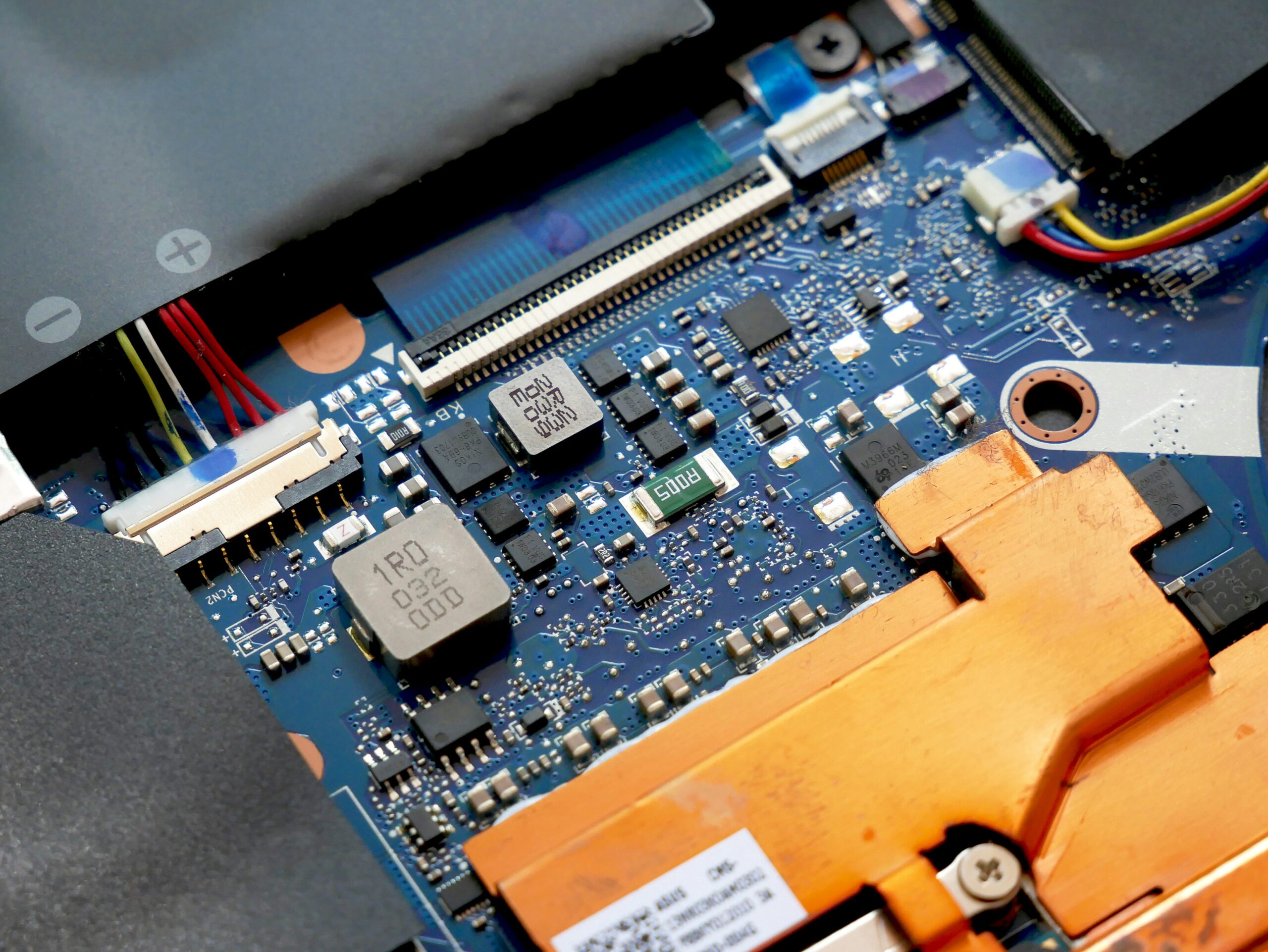
Photo by Vishnu Mohanan on Unsplash


